One of the issues from my first day with DesignSpark PCB was the fact that my titleblock printout didn’t come out as expected. All of the text was shifted down a little and was the wrong size. I did a little more investigation and it turns out that if you use a stroke font instead of a True Type, the alignment doesn’t change when printing. The font size is also the same. However, in order to use stroke fonts you need to declare them in the design technology file for every size and type you intend to use. Even though it looks like you can edit the size of a stroke font by just clicking on it, you can’t.
The next step in my project is to draw the schematic. That was easy – the drawing and placement tools are pretty straight forward. Here’s what I ended up with.

And here’s a closeup of the actual schematic.

Now to try and make a PCB. The first step is to make a frame like I did before, except I want it to be 8.5×11 instead of 11×17. I find that 90% of my boards are fairly small (< 6in x 6in) and that will keep the print out from getting too small. Based on my experience with the schematic frame, I’m just going to make a library component for it instead of trying to do it directly in the PCB technology file.
The first step was to copy the default technology file with 2 signal layers. Except that I had changed the default technology file path for my schematic template file and had no idea where to find the PCB templates. Turns out the DesignSpark PCB puts all of the ltechnology files in C:\Documents and Settings\All Users\Documents\DesignSpark PCB\Technology. Yay search!
Unfortunately the PCB technology file needed a lot of editing which I did before I made the frame. The default on was set up for 2 layers, but was missing assembly, solder mask and past mask layers which I added. I also design all my boards in metric units which I changed. Turns out that all of this editing wasn’t required. When you make a new PCB there’s a wizard that asks you how many layers you want, paste masks, etc. For some reason the option to use the layers defined in the technology file was grayed out. I guess this means that I have to give up on have assembly drawing and placement layers in my components like I’m used to for Altium Designer. Not a huge issue though.
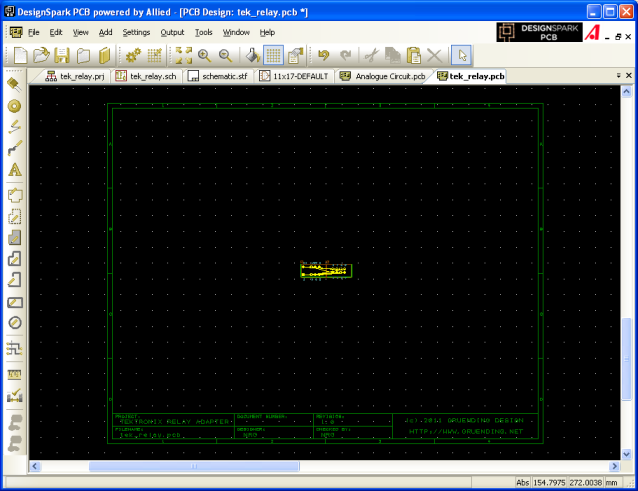
I also noticed that the wizard didn’t let me import a board shape from another file. The “Use Board Outline From Chosen Technology File” and “Copy Board Outline From Another File” options were grayed out. Once I made my template I tried printing it and it worked fine when I used the pdf output option. I didn’t try printing to the printer. I also didn’t try true type fonts. Here’s what the PCB file ended up looking like:

And here’s a close up of the board:

I first thought that you could manually add the PCB file to the project using File->New. But that’s not correct – you need to use Tools->Translate to PCB instead. This may be an issue for multiple page sheet designs that I’ll have to try another time. If you make a mistake on the board size like I did you pretty much need to delete the board outline and start over. It’s kind of frustrating that you can’t edit the coordinates of the lines by hand after they’ve been placed.
I also realized that DesignSpark didn’t like how I make the footprint for K1. I had originally designed it with the extra 2 pins as a generic footprint but only defined 8 in the schematic symbol. DesignSpark automatically assigned pin numbers to the unused pins (2 and 6) which made everything weird. There doesn’t seem to be a way to add the correct pin numbers for pins that don’t have a schematic and PCB pin. So I just deleted the extra pins on the footprint and updated the library.
Now I needed to update the PCB footprint. I started by updating the schematic symbol and then trying to push the changes to the PCB like I would with Alitum Designer. Except that when I tried Tools->Forward Design Changes the footprint didn’t change. Tools->Translate to PCB wanted to replace the whole PCB file which I definitely didn’t want. So I selected the part in the PCB and updated it there which worked.
But this behaviour worried me a bit. What would happen if I added or removed components later? So I added another relay to the schematic to try. I did Tools->Forward Design Changes and nothing happened. I tried Tools->Schematic/PCB Check and no errors were found. I was getting really worried so I added a wire connection to the new relay and then the PCB was correctly updated. I deleted the new relay and it worked too. Whew!
So far so good. It’s been a bumpy ride, but so far DesignSpark PCB will work for me. Next we’ll try routing the board. I don’t use autorouters for a bunch of reasons so I’ll be doing it by hand.